Multiplexer

I. Intended Learning Objectives
At the end of the tutorial, the readers should be able to:
1. Explain the operation of a multiplexer.
2. Construct the digital circuit using CircuitSim for a multiplexer; and,
3. Perform simulation of the operation of a multiplexer.
II. Requirements
The readers should have a desktop PC or laptop (Win 7, 8, or 10) with an installed CircuitSim simulator to be able to effectively learn the concepts and procedures that will be discussed in this tutorial. Readers will be able to download a copy of the app at ra4king.github.io/CircuitSim/ download page or visit its official Github repository at ra4king/CircuitSim.
III. Difficulty
Intermediate
IV. Introduction to Multiplexers
The process of transmitting a large number of information over a smaller number of channels is called multiplexing. . A digital multiplexer is a combinational circuit that selects one binary information from a set of input lines and directs it to a unitary output line. A set of selection line enables selection of the input line. In designing a multiplexing circuit, we will set 2^n input lines and n selection lines with a unitary output line. For example, we wan to design a 4 to line multiplexer. So, we need to have 4 input line, 2 selection line and 1 output line. The multiplexing operation is done by configuring a circuit that has a 4 set of AND gate which is feed to an OR gate. The AND gate will have three input lines where the two of which is dedicated to a selection line for the multiplexing operations.
Figure 1: Flowchart for the 4 to line multiplexing operation
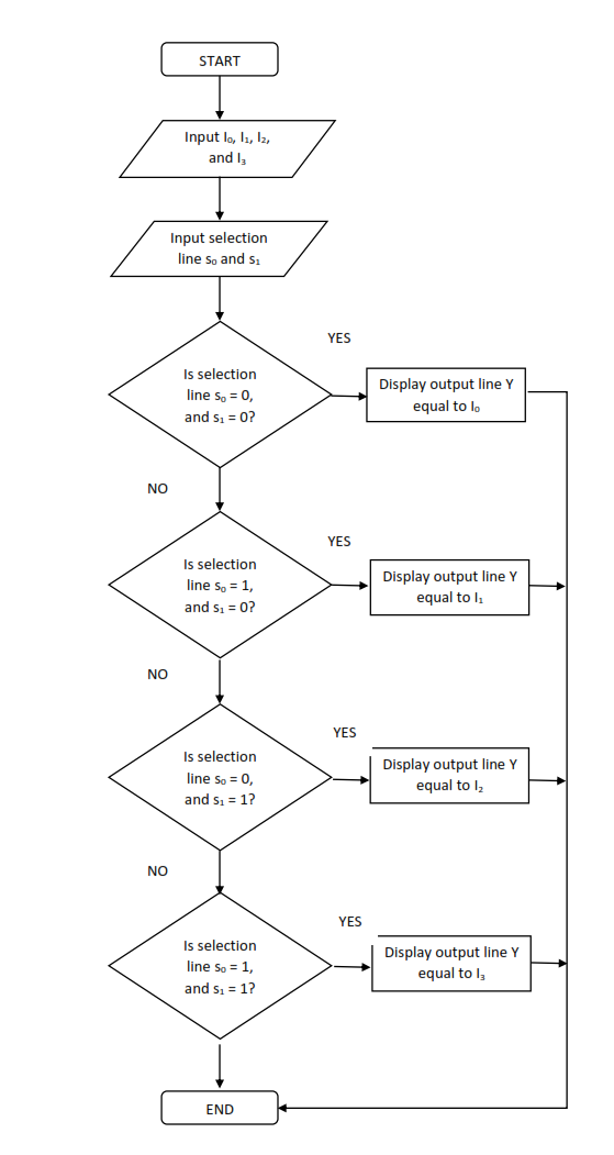
In this tutorial, we will make 4 to 1 line multiplexer whose operation is presented in the design flowchart in figure 1. We start establishing 4 set of input and 2 set of selection line. This sets of inputs is manipulated using a cascaded design of AND and OR gate. The AND gate will receive one input from the set of input line( I0, I1, I2, and I3) and the two set of selection line. The selection line designated as s0 and s1 will enable the input. Selection lines are connected to all AND gate which receives different input lines. The output of the AND gates is then sum up on an OR gate. This configurations enables us to do the conditional statements that can seen on our design flowchart.
Table 1: Truth Table for 4 to 1 line multiplexer

V. Multiplexer implementation on CircuitSim
We have discussed earlier the operation of a multiplexer. At the same time, we discussed the construction of a basic multiplexer circuit. It is constructed with sets of AND gate with the three terminal input. One input is designated to a unique bit value as I0, I1, I2, and I3. The other two input terminal of the AND gates is uniformly connected to the designated selection s0 and s1. We open a new circuit editor in the CircuitSim. Select four set of AND gate with each having a designated input element label accordingly from top to bottom as I0, I1, I2, and I3. The AND gate can be located at the gate tab on the apps.

The problem now is that the CircuitSim's AND gate only have two terminal for the input. So, you need to click on each AND gate, and edit the terminal number that can be located below the component library. We will do this steps until we have finished configuring a all AND gate with three terminal each. We have now configured 4 set of three terminal AND gate. We will now add input element labeled accordingly from top to bottom as I0, I1, I2, and I3.

Next, we add the the input element for the selection line and define it as s0 and s1. This is connected to all remaining terminals in each AND gates. This serve as the enabling bit for the input line to be displayed at the output line. Simply adding this enabling inputs s0 ans s1 does not give the multiplexing operations. So, we need to add an inverter between so and s1 but it is not connected to all terminal in the available AND gates. Inverted selection line s0 is connected to the first two AND gate, and s1 is to the primary and the third AND gate. Regular bit for s0 is connected to the second and fourth AND gates; and, s1 is connected to third and fourth AND gates. This will complete the conditional statement I have presented earlier on the design flowchart.

The output from the AND gates is feed to a four terminal OR gate to establish the final bit to be displayed. Now, we add the output element labeled as Y. To finalize the constructed circuit on the CircuitSim, we need to rename the circuit from new circuit to multiplexer.

On CircuitSim, we have configured and simulated a multiplexer. To further elaborate the application of a multiplexer, we will incorporate a shift register to automate the shifting of input line and the selection line bit. First, we need to configure a shift register as a new circuit component. You can read my other tutorial on how to build a shift register. For a brief review, a shift register is constructed using an array of d flip-flops connected in a manner that the preceding output is connected to the immediate input of the succeeding D flip-flop. Now, connect for two set of shift register to the multiplexer input lines in an alternate manner. So, register A connected to input I0 and I2, and the remaining input lines connected to register B. Another set of shift register is connected to the selection line where one will be the inverted value of the other.

Connect one clock pulse for both register. At the same time connect two set of serial input elements for both register. To finalize the circuit, connect the output element at terminal Y of the mux.

The circuit shifts the 2 bit values from the shift register and process the 4 bit information to a 1 bit information using the multiplexer. A logic 1 output at Y is possible only when input A, B, and S is equal to logic 1. Any change state from 1 to 0 in the enabling inputs the value of the output Y is change to 0.
| VI. Simulation of the Multiplexer operation |
|---|
We have now created the a multiplexer and do an advance application by combining a shift register to it. All output simulation from both circuit is presented below. To start the simulation, simply click simulation > simulation enable and also clock enable. In the running simulation as shown, we can observe a that the value of Y at is similar to the truth table I have presented earlier. In the simulation, we follow the initial steps as presented in the flowchart earlier. We input values to I0, I1, i2, and I3. At the same time, we need to toggle between different values at s0 and s1. Simulation 1: Multiplexer Logic CircuitFor the second simulation, we input logic 1 values for all input and, next change any values to 0. This is done to full present the characteristics of the circuit.You can see the recorded simulation on the video below. Simulation 2: Multiplexer application with a shift register |
VIII. Summary
In this tutorial, we start by understanding the operation of a multiplexer. We have learned that multiplexing operation is processing a large number of information channel to a smaller channel. The circuit is constructed by arranging an AND and OR gate so that the conditional statements as presented on figure 1 is achieve. The AND gate is connected to a distinct input, and a common s0 and s1 bit values as well as its inverse. The OR gates finalize the configurations which helps decide the final 1 bit value to be displayed or outputted on terminal Y. We have conduct a simulation and present a copy of the recorded simulation in the prior section of this tutorial. Furthermore, we have done a more complex circuit where we applied the multiplexer with a shift register. This circuit shifts the 2 bit serial input from the shift register and process a 4 bit information channel to a 1 bit information channel using the multiplexer. Thus, a logic 1 output at Y terminal is possible only when input A, B, and S is equal to logic 1. Any change state from 1 to 0 in the enabling inputs the value of the output Y is change to 0. The operation inside the multiplexer on the second simulation can be viewed from the first simulation.
VIII. Reference
Conceptual Reference: Morris Mano, Digital Design, 3rd Edition
Image and Video Source: All videos and images use in this tutorial is recorded and captured by the author. Otherwise, it is specified in the text.
IX. Curriculum
You can browse my other tutorial for digital circuits implemented using CircuitSim from the following links bellow.
1. Binary Ripple Counter
2. Shift Register
3. Serial Binary Adder
Posted on Utopian.io - Rewarding Open Source Contributors
Thank you for the contribution. It has been approved.
You can contact us on Discord.
[utopian-moderator]
Thank you for your time moderating and approving my post, @portugalcoin!
Hey @juecoree I am @utopian-io. I have just upvoted you!
Achievements
Community-Driven Witness!
I am the first and only Steem Community-Driven Witness. Participate on Discord. Lets GROW TOGETHER!
Up-vote this comment to grow my power and help Open Source contributions like this one. Want to chat? Join me on Discord https://discord.gg/Pc8HG9x
Awesome! Nice post juecoree
Your article is well written, and I will continue to pay attention to you.
I want to ask you how to do this steemit?
What do you do to make your steemit get such a high income?
Sincerely ask for you, thank you!
If u want check my article about 등갈비 김치찜!!!!
You can find the article here 등갈비 김치찜!!!!
I will follow you juecoree