Failure Analysis with Fred Femto Field (Part 6)
Failure Analysis: The mighty TEM
Hey dear electrons! Fred Femto Field here! Hope You all had a great weekend!
In the last post, I told You that I would be continuing with TEM (Transmission Electron Microscopy), so here we go!
Transmission electron microscopes (TEM) use a beam of electrons to visualize specimens and generate a highly-magnified image. TEMs can magnify objects up to 2 million times The high energy beam, focus in a very thin sample, and the interactions between the electrons and the atoms can be used to observe features such as the crystal structure and features in the structure like dislocations and grain boundaries. It can be used to study the growth of layers, their composition and defects in semiconductors. In the quantic field, it might be used to analyze the quality, shape, size and density of quantum wells, wires and dots. Chemical analysis can also be performed.
How does TEM work?
TEM is composed by an electron gun at the top, which emits electrons that travel through the microscope’s vacuum tube. TEM employs an electromagnetic lens which focuses the electrons into a very fine beam. This beam then passes through the specimen, which is very thin, and the electrons either scatter or hit a fluorescent screen or a digital camera at the bottom of the microscope. The fluorescent screen, is an instrument consisting of a surface containing chemicals called phosphors that produce light, when hit by X rays or gamma rays, allowing the user to see an image. The darker areas of the image represent those areas of the sample that fewer electrons are transmitted through while the lighter areas of the image represent those areas of the sample that more electrons were transmitted through.
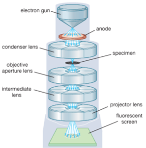
Image's Source
The TEM is used for obtaining image and chemical information about the nano and microstructure of all types of materials, ranging from metals and ceramics to soft biomaterials. 2D and 3D imaging of the structures is possible as well as the mapping of electric and magnetic fields. TEM’s samples require a thickness of less than 100 nm. Also, since the microscope operates under high vacuum, samples have to be dry and they also need to withstand the exposure to the high energy electron beam.

Image's Source
Quantum Dots in the image above! Amazing right?
No more to tell about TEM at the moment... Next post on FIB! See You soon!!!
Cheers from 10-15 !!
References:
- https://warwick.ac.uk/fac/sci/physics/current/postgraduate/regs/mpagswarwick/ex5/techniques/structural/tem/
- https://www.britannica.com/technology/transmission-electron-microscope
- https://www.ccber.ucsb.edu/collections-botanical-collections-plant-anatomy/transmission-electron-microscope
- https://www.britannica.com/technology/fluoroscope
@tipu curate
Upvoted 👌 (Mana: 10/20 - need recharge?)
Congratulations @heteronimo! You have completed the following achievement on the Steem blockchain and have been rewarded with new badge(s) :
You can view your badges on your Steem Board and compare to others on the Steem Ranking
If you no longer want to receive notifications, reply to this comment with the word
STOP