AMD Could Solve Memory Bottlenecks of its MCM CPUs by Disintegrating the Northbridge
AMD sprung back to competitiveness in the datacenter market with its EPYC enterprise processors, which are multi-chip modules of up to four 8-core dies. Each die has its own integrated northbridge, which controls 2-channel DDR4 memory, and a 32-lane PCI-Express gen 3.0 root complex. In applications that can not only utilize more cores, but also that are memory bandwidth intensive, this approach to non-localized memory presents design bottlenecks. The Ryzen Threadripper WX family highlights many of these bottlenecks, where video encoding benchmarks that are memory-intensive see performance drops as dies without direct access to I/O are starved of memory bandwidth. AMD's solution to this problem is by designing CPU dies with a disabled northbridge (the part of the die with memory controllers and PCIe root complex). This solution could be implemented in its upcoming 2nd generation EPYC processors, codenamed "Rome."
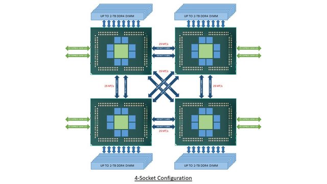
With its "Zen 2" generation, AMD could develop CPU dies in which the integrated northrbidge can be completely disabled (just like the "compute dies" on Threadripper WX processors, which don't have direct memory/PCIe access relying entirely on InfinityFabric). These dies talk to an external die called "System Controller" over a broader InfinityFabric interface. AMD's next-generation MCMs could see a centralized System Controller die that's surrounded by CPU dies, which could all be sitting on a silicon interposer, the same kind found on "Vega 10" and "Fiji" GPUs. An interposer is a silicon die that facilitates high-density microscopic wiring between dies in an MCM. These explosive speculative details and more were put out by Singapore-based @chiakokhua, aka The Retired Engineer, a retired VLSI engineer, who drew block diagrams himself.
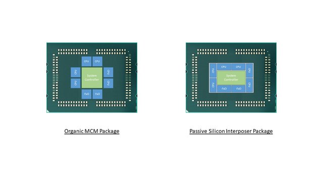
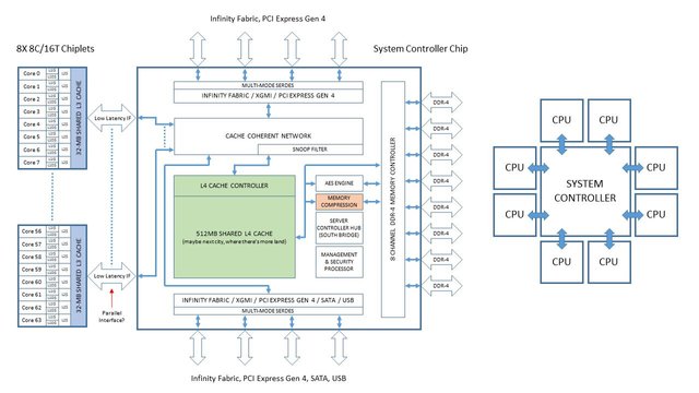
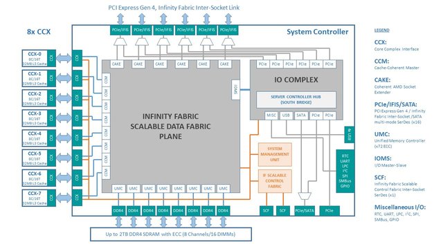
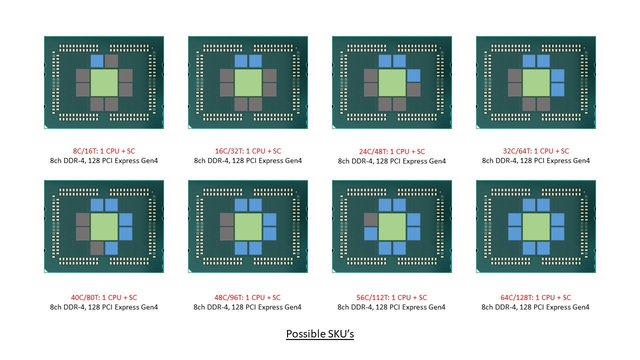
The System Controller die serves as town-square for the entire processor, and packs a monolithic 8-channel DDR4 memory controller that can address up to 2 TB of ECC memory. Unlike current-generation EPYC processors, this memory interface is truly monolithic, much like Intel's implementation. The System Controller also features a PCI-Express gen 4.0 x96 root-complex, which can drive up to six graphics cards with x16 bandwidth, or up to twelve at x8. The die also integrates the southbridge, known as Server Controller Hub, which puts out common I/O interfaces such as SATA, USB, and other legacy low-bandwidth I/O, in addition to some more PCIe lanes. There could still be external "chipset" on the platform that puts out more connectivity.
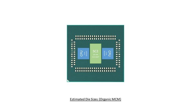
The Retired Engineer goes on to speculate that AMD could even design its socket AM4 products as MCMs of two CPU dies sharing a System Controller die; but cautioned to take it with "a bowl of salt." This is unlikely given that the client-segment has wafer-thin margins compared to enterprise, and AMD would want to build single-die products - ones in which the integrated northbridge isn't disabled. Still, that doesn't completely discount the possibility of a 2-die MCM for "high-margin" SKUs that AMD can sell around $500. In such cases, the System Controller die could be leaner, with fewer InfinityFabric links, a 2-channel memory I/O, and a 32-lane PCIe gen 4.0 root.
AMD will debut the "Rome" MCM within 2018.
Hi! I am a robot. I just upvoted you! I found similar content that readers might be interested in:
https://www.techpowerup.com/249108/amd-could-solve-memory-bottlenecks-of-its-mcm-cpus-by-disintegrating-the-northbridge
Hi @djxheadhunterz, I'm @checky ! While checking the mentions made in this post I noticed that @chiakokhua doesn't exist on Steem. Maybe you made a typo ?
If you found this comment useful, consider upvoting it to help keep this bot running. You can see a list of all available commands by replying with
!help.Congratulations @djxheadhunterz! You received a personal award!
You can view your badges on your Steem Board and compare to others on the Steem Ranking
Vote for @Steemitboard as a witness to get one more award and increased upvotes!