🔋 NiCd Battery Charger Circuit Diagram (Using NE555 IC)
Assalamualaikum Everyone. I am @imranhassan From #Bangladesh
.png) |
|---|
| 🛠️ Components used and their functions |
|---|
🔹 NE555 Timer IC
 |
|---|
- 👉 Acts as the main control system of the circuit. This IC provides timing signals, which helps in the subsequent political control process.
🔸 78L05 Voltage Regulator IC
 |
|---|
- 👉 Regulates the input voltage to 5V. This IC ensures that the 12V input code is restored and provides a 5V link voltage to the signal battery.
🔹 1N4148 diodes (total 4)
 |
|---|
- 👉 Used in the signal route to block reverse current. It prevents current from returning to the IC or circuit from the battery side so that the circuit is not damaged.
🔸 Resistor (10kΩ ×2, 680Ω ×1)
 |
|---|
- 10kΩ (2): Pins 6 and 2 of NE555 are used for timing configuration. 680Ω (1): Limits the LED; the current does not burn the LED.
🔹 Capacitor (10nF ×2, 1μF ×2)
 |
|---|
- 10nF (2): As a filter in the control voltage and ground part of the NE555 IC. 1μF (2): To filter the out signal and maintain the capacity of the networking line.
🔸 LED
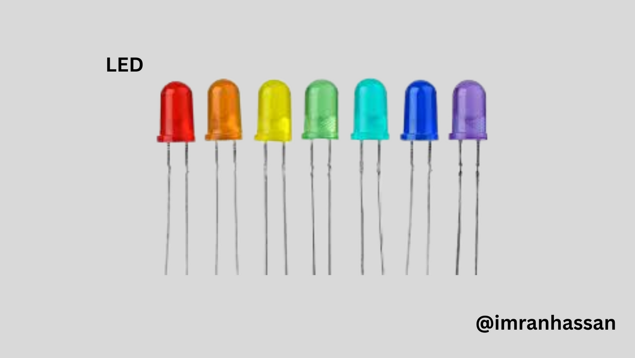 |
|---|
- Lights up during news discussion. Works as an indicator.
🔹 NiCd battery
 |
|---|
- 👉 This is the main load of the circuit. Through this circuit, the battery gets power, and the LED provides security.
🔸 12V Power Supply
 |
|---|
- 👉 Input for circuit formation. In this circuit, the voltage is calculated, and all the voltages are regulated and fed to the battery. Using these materials, the circuit is formed, developed and taught.
| 🔹 Step 1: Preparation for drawing the diagram |
|---|
 |
|---|
In the first step, I took the necessary materials for drawing the diagram, such as a scale, a black ballpoint pen, and green, red and blue pens—which I have shown in the picture. Using correct lines, different parts in different colours and maintaining correct sizes are very important in drawing the circuit, especially when we are learning to draw by hand.
| 🔹 Step 2: Power Supply Timer Configuration and Signal Preparation |
|---|
 |
|---|
In this step, I mainly drew the timing configuration of the NE555 Timer IC and the output signal generation part. This part works like the brain of the circuit because from here the signal for the next charging part is generated.
🔸 Power Supply Setup:
I have used a 12-volt DC power supply in the circuit, which is fed through two 1N4148 diodes. The diodes protect the two circuits from reverse current.
🔸 Trigger and Threshold Setup:
I have used two 10kΩ resistors with Pin 6 (Threshold) and Pin 2 (Trigger). These act as timing resistors and keep the NE555 IC in astable mode. I have connected these two pins together so that the timing signal is generated properly.
🔸 Control Voltage Pin:
I have connected a 10 nF capacitor to ground with Pin 5 (Control Voltage). This helps in keeping the internal reference voltage of the IC constant.
🔸 Discharge and Reset Pin:
I have connected Pin 4 (Reset) directly to VCC (Pin 8) so that the timer is always active. Pin 7 (Discharge) discharges the timing capacitor and turns off the signal.
🔸 Ground and VCC:
Pin 1 is connected to ground and Pin 8 to VCC so that the circuit operates properly.
Summary:
In this step, I have basically created a timing configuration, which will provide a fixed-length output signal for the charging process. From here, through Pin 3 (Output), we will create the switching and charging control part in the next step.
| 🔹 Step 3: Output Signal Filtering and Starting to Create a Charging Path |
|---|
 |
|---|
In this step, I created a safe and stable path to send the output signal from Pin 3 (Output) of the NE555 Timer IC to the battery. Basically, from this part, the circuit is ready to start charging.
🔸 Adding a 1μF 16V Capacitor:
I first used a 1 microfarad capacitor with Pin 3, which filters the output signal. This helps in making the timing signal of the circuit more stable and clean.
🔸 Using a 1N4148 Diode:
Then I added a 1N4148 diode, whose function is to prevent reverse current coming from the battery side. This is essential for the safety of the circuit.
🔸 Starting the Charging Line:
After this diode, a charging line starts, which will go to the LED indicator and battery in Step 4. This is our output path, which I mentioned as part of the end of Step 2.
Summary:
In this step, the output signal generated by the NE555 is properly processed and prepared for sending to the battery. This output line is safe, filtered and protected from signal loss or backflow.
| 🔹 Step 4: Voltage Regulation, LED Indicator and Final Battery Output |
|---|
 |
|---|
In this step, I have completed the main output part of the circuit, where the charging current goes to the battery. At the same time, an LED indicator and a voltage regulator (78L05) have been connected to make the charging system more safe and reliable.
🔸 Voltage Regulator IC – 78L05:
The signal coming from Pin 3 is filtered through two diodes and a capacitor and enters a 78L05 Voltage Regulator IC. If 12V or more is input to this IC circuit, it regulates it and gives a correct 5V DC output, which is safe for battery charging.
🔸 LED Indicator & 680Ω Resistor:
I have connected an LED to the 5V output line coming out of the 78L05 through a 680Ω resistor. If the LED lights up, it will be understood that the battery is charging. The resistor limits the current of the LED and extends the life of the LED.
🔸 Battery Output Line:
Finally, I have given an “Output to NiCd Battery” label to the positive end of the battery and connected the negative end to the ground line. This step completes the output part of the circuit, where it is.
| NE555 Timer IC Pin Configuration (8 Pins): |
|---|
| Pin Number | Name | Function |
|---|---|---|
| Pin 1 | GND (Ground) | Connected to the ground or negative line of the circuit. |
| Pin 2 | Trigger | When the voltage on this pin is low, the timer starts. |
| Pin 3 | Output | When the timer is on, the output signal comes out from here. |
| Pin 4 | Reset | When low (low), the timer stops. Usually connected to VCC. |
| Pin 5 | Control Voltage | To control the internal threshold. Usually connected to ground with a 0.01 µF capacitor. |
| Pin 6 | Threshold | When a certain voltage is reached on this pin, the timer stops (the output is Low). |
| Pin 7 | Discharge | Used to discharge the timing capacitor. |
| Pin 8 | VCC (Power Supply) | Positive power supply up to 5V–15V is provided. |
| ✅ Conclusion: |
|---|
 |
|---|
I created this project purely for educational purposes so that even beginners can confidently move forward in the world of electronics. This circuit includes timing control, LED indication, reverse current prevention, and a safe charging system—all of which together create a great hands-on learning opportunity.
.gif)
| Photography Details | 📱 Device: Walton Xanon90 | 📍 Location: Narayanganj, Bangladesh | 📷 Captured By: @imranhassan |
|---|
https://x.com/ImranHosen98536/status/1927062338177319174