How are you all friends? I hope you are well. I am also well. Today I will show you a DC voltage doubler circuit diagram. It will produce 24V DC output from 12V DC input and will be used to get high voltage in various applications. I have made this circuit using an NE555 timer IC.
Edited with Canva.
| Parts used and functionality: |
|---|
NE555 timer IC:
Edited with Canva.
It is used for timing and signal control.
Resistance:
For voltage division and signal control.
Capacitors:
Used to store voltage and smooth the signal.
Diode:
Used to filter and discharge the signal.
12V Battery:
| Used to supply power to the circuit. |
|---|
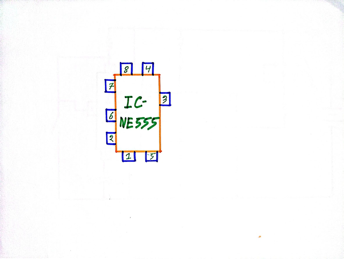
| First, I took the 555 timer IC and figured out its pinouts. |
|---|
Pin 1 Ground: Zero voltage of the IC. Pin 2 Trigger: Used to trigger the signal. Pin 3 Output: Provides the output signal. Pin 4 Reset: Used to reset or restart the IC. Pin 5 Control Voltage Input Pin: This helps in controlling the performance of the IC. Pin 6 Threshold Pin: Used for timing and signal control. Pin 7 Discharge: Pin used to discharge the charge of the capacitor. Pin 8 Power Supply: The power supply pin supplies voltage to the circuit.
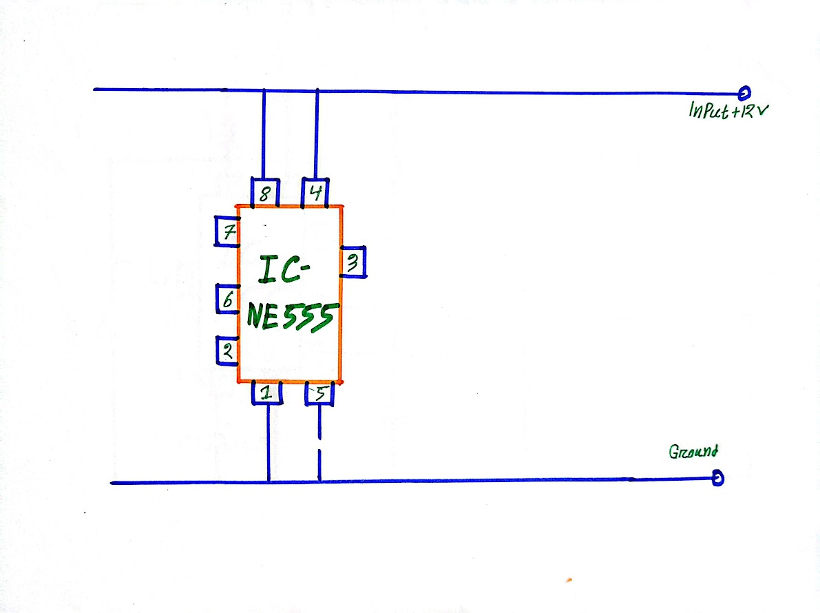
First I took the pin out of the NE555 IC correctly and then connected pin 1 and 5 to ground and pin 8 and 4 to the positive line.
| Step 2: Resistance and Capacitor Connection: |
|---|
Then I connected resistance 1 – 15K to pin 7 and resistance 2 – 27K to pin 6 and pin 2. Then, I drew capacitor 1 (-0.01 µF) and capacitor 2 (0.01 µF) to control the voltage and smooth the signal.
| Step 3: Output Connection: |
|---|
Then I connected diode 1 (1N4001) and diode 2 (1N4001) to output pin 3. Then I connected capacitor 3 – 330 µF to ensure a stable signal. Then capacitor 4 (330 µF) and capacitor 5 (470 µF) help in maintaining the output voltage. With these three steps, my entire circuit is complete, and it is now functional.
This circuit produces 24V DC output from a 12V DC input. All the parts of the circuit are connected properly, and voltage doubling is working effectively. Then I took a selfie with the circuit design and wrote the name of the community as my username.
| S.no | Component Name | Value | Qty |
|---|
| 1 | Timer IC | NE555 | 1 |
| 2 | Resistor | 15K, 27K | 1, 1 |
| 3 | Diode | 1N4001 | 2 |
| 4 | Capacitor | 0.01uF, 330uF, 470uF | 2, 2, 1 |
| 5 | Battery | 12V | 1 |
.gif)
🟩 Thank you for reading my post and giving your valuable time. Stay well and stay healthy. God bless you.
🟩 |
|---|
| Photography Details | 📱 Device: Walton Xanon90 | 📍 Location: Narayanganj, Bangladesh | 📷 Captured By: @imranhassan |
|---|
.png)


.gif)
https://x.com/ImranHosen98536/status/1943595169606959505