Circuit design using "Multisim"(Regulated voltage source)
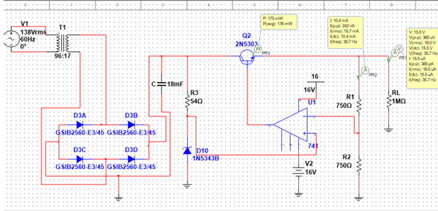
I am a student of electronic engineering from the Simón Bolívar University of Venezuela (USB), a few quarters ago I was studying the subject "Electronics of industrial acquisition and processing systems 2" where we were assigned the task of designing a voltage source by regulation Continue with serial configuration.
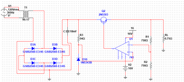
The requested values of current and maximum voltage are: Vo = 15V and Io = 20A. The design of the voltage source by continuous regulation in series configuration with the following components was implemented:
T1: 2N5303
PMax = 200W; Ic = 20A; Vcc = 4V; VceSat = 2V; VbeSat = 2,5V.
Diodes: A,B,C,D: GSIB2550-E3/45
Vp = 200V; VrmsMax= 140Vrms; Imax = 350A
Diode: Zener: 1N5343B:
Vz = 7,5V; IzMin = 175mA; Pmax = 5W; IzMax = 140Vrms.
Then the calculations used to design it:
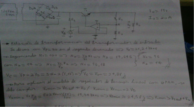
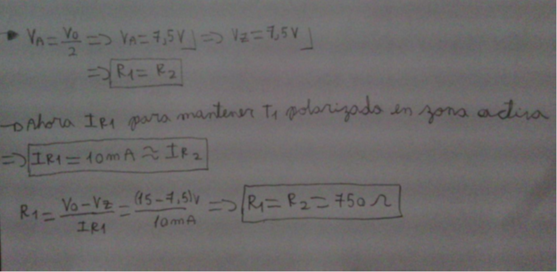
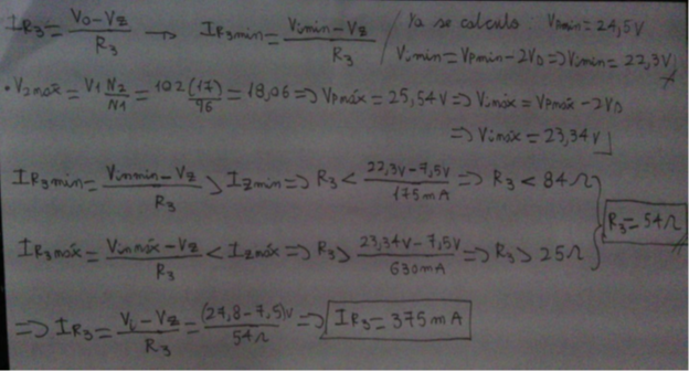
Once the values were obtained, the circuit was assembled in MULTISIM:

Simulation with maximum current:
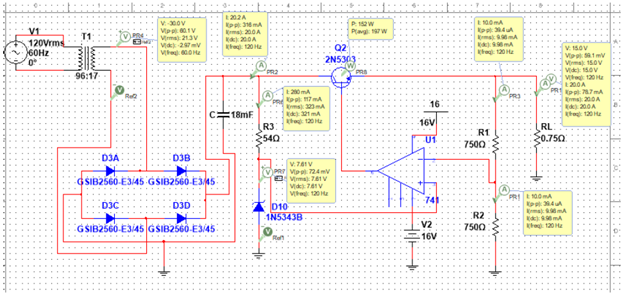
It is observed how the values calculated by hand closely approximate those obtained in the simulation: With a 0.2% error for IR1 and IR2 and a 10% error in IR3. A voltage of 15V and a current of 20A are observed at the output, which are the maximum values specified.
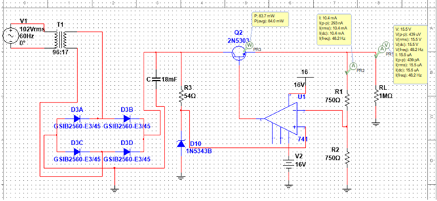
Simulation with minimum current (1M resistor was used).

By increasing the resistance to 1M, it can be seen that the voltage is still close to 15V, it only increases by 0.5V, which indicates that the source behaves correctly in case of load variations.
Short Circuit Simulation:
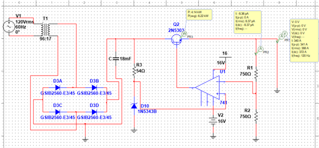
An attempt was made to implement the Overcurrent protection, but no diodes were found that complied with the requirements, as there was a short circuit at the output, a large amount of current was observed in it, and a large power dissipated by the transistor which indicates that it will not take long to get damaged.
Minimum input voltage according to the indicated line regulation:
At minimum input voltages 120Vrms - 15% = 102Vrms. The regulator continues to perform its function and continues to display an output of 15.5V, a value very close to the 15V requested for all RL values greater than the maximum condition of RL = 0.75 Ohm where 15V and 20A are observed.

Maximum input voltage according to indicated line regulation:
At maximum input voltages 120Vrms + 15% = 138Vrms. The regulator continues to perform its function and continues to display an output of 15.5V, a value very close to the 15V requested for all RL values greater than the maximum condition of RL = 0.75 Ohm where 15V and 20A are observed.
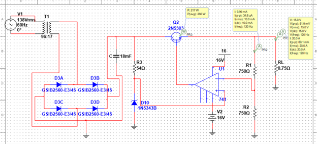
The regulation of the output voltage is given by: 𝑉𝑜𝑆𝐶 − 𝑉𝑜𝐶𝑀𝐶𝑉𝑜𝐶𝑀𝐶 ∗ 100 = 0−1515 * 100 = 1%Which meets the minimum requested.
Results:
It was possible to successfully design the voltage source so that in any case it would throw 15V at the output or very close values that stopped changing once the critical condition of RL was exceeded, these results remained the same if the line regulation voltage was varied , which indicates the proper functioning of the circuit, however, it was not possible to adapt the overcurrent protection so the design is inefficient since it will fail if a fault occurs that produces a short circuit.
Hello @orbital753, thank you for sharing this creative work! We just stopped by to say that you've been upvoted by the @creativecrypto magazine. The Creative Crypto is all about art on the blockchain and learning from creatives like you. Looking forward to crossing paths again soon. Steem on!